PCB Layout:
Mechanical Architecture, PCB Design & 3D Modeling
Following our thorough review of your product’s circuit schematics, we undertake Printed Circuit Board layout using the latest version of Altium Designer. PCBs may range from simple single boards, through to multi-board stacks with complex mechanical constraints.
We work closely with your mechanical or industrial designers to ensure that the resultant PCB layout fits perfectly into its enclosure. Alternatively, we can assist you in the design or selection of a suitable enclosure, or team up with industrial designers to develop an enclosure design to suit your needs.
Genesys has in-house mechanical design capability and 3D-printer based fabrication capability. This allows the generation of prototype-level mechanical PCBs and custom enclosures, and mechanical assemblies.
CAD & CAM
We are an Authorised Altium Service Bureau Partner, and use Altium’s 3D modeling facilities to provide continual feedback to the design team to ensure optimum fit. The gallery below shows an illustrative example of the process used and how the mechanical design integrally develops, with the various views and models that are utilised.
Including the enclosure 3D model with these views, we end up with a completely detailed 3D model that serves as a sound pre-fabrication verification of the product's mechanics, that is closely representative of the final product form.
Complexity
We can develop PCB’s of any size, complexity, density, technology and number of layers, including high speed digital, BGA, RF and mains-voltage layouts. We have developed boards with layer stacks up to 16-layers, blind and buried vias, micro-vias, fine-pitch devices, high density BGA’s and track clearances down to 0.05mm.
We have an extensive library of production-proven PCB component footprints, to maximise production yield and product reliability. We know all of the tricks required to achieve EMC compliance and mains safety compliance on the first pass. On completion, PCB layouts are thoroughly reviewed, and panelised ready for manufacture.

PCB Layout: mechanical architecture, PCB design & 3D
modeling.
Other Genesys Services:
-
Sketch
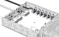
A rough concept capturing visuals & form factor, that is mechanically, electrically & electronically feasible.
-
2D DXF
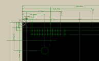
Spawned from a refined 3D mechanical model: 2D CAD outline & mounting drawings of each assembly PCB.
-
2D PCB
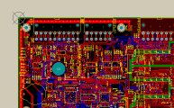
Detailed PCB partitioning by subcircuit and/or function, connector & component placement and tracking.
-
3D PCB
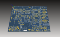
A virtual representation of the final bare PCB provides an excellent 'sanity check' of visible PCB-only detail.
-
3D PCB Subassembly
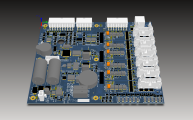
A virtual PCB subassembly allows preview of PCB component-component & component-board mechanics.
-
3D Assembly
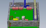
Seamless importing of the PCB sub-assembly into the 3D mechanical model, confirming PCB clearance.
-
Final PCB Subassembly
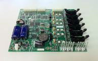
No surprises: the final real populated PCB subassembly, exactly as it has been conceived and designed.
-
Final Assembly
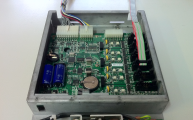
The perfect fit - again, no surprises. "One Pass To Production™" is the Genesys reality.

